TEM and Electron Diffraction
Keith Leonard, PhD (1999)
U. Cincinnati
Electron Microscopes:
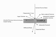
Electron microscopes, such as the scanning electron microscope (SEM) and transmission electron microscope (TEM) are instruments used in the analysis of materials on a scale much smaller than possible by optical microscopy. The electron microscopes also use the many interactions that the electron beam has on the sample (Figure 1) to produce various imaging and diffraction modes that can be used to analyze the material down to the atomic scale. A SEM uses the electrons that are scattered off of the sample surface to produce images of the sample. In a TEM, the electron beam passes through the sample and produces an image using the transmitted electron beam; which contains both diffracted and unscattered electrons. Detectors in both SEM and TEM instruments collect the characteristic x-rays that are generated from the sample to allow for compositional analysis of the material. This type of x-ray production in the sample is the same principle as that of the generation of x-rays used in x-ray diffraction instruments.
Figure 1. Electron beam/sample interactions.
Uses of SEM:
-surface topography and analysis of fracture surfaces
-imaging regions or phases of different chemical composition
-composition analysis of individual phases
Uses of TEM:
-identifying the phases and crystal structures present in the material
-characterizing and identifying defects (antiphase boundaries, dislocations, stacking faults) in the crystal structure and to determine modes of deformation (identifying the slip systems of a material or mode of failure)
-determining site occupancy preferences of the atoms in the crystal structures
-determining the growth directions of precipitates or lamella in the material and the type of interfaces between different phases (i.e. coherent, semi-coherent and incoherent)
-imaging atomic planes and defects in packing associated with dislocations or interfaces
-compositional analysis of individual phases
Limitation of TEM: Sample size and preparation. The material must be less than 200 nm thick in order to pass the electron beam through. So you are only observing a very small portion of the material.
Electron vs. X-ray Diffraction:
l electrons (200 kV) = 0.0251 Å
l x-rays (CuKa) = 1.5418 Å
Ewald’s Sphere construction:
radius of Ewald’s Sphere ~ 1/l
if the material of interest has a lattice parameter of ao = 3.6Å, a*=0.278Å-1
1/
l electron = 39.8 Å-11/
l x-ray = 0.65 Å-1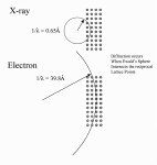
Figure 2. Ewald’s Sphere construction for electron and X-ray radiation.
Because the radius of the Ewald’s sphere (1/
l) of the electron beam is large in comparison to the reciprocal lattice, (along with beam convergence and small variations in l) you are assured to produce diffraction off multiple planes. Whereas in XRD, it can very difficult to produce diffraction from a perfect single crystal. This is why in XRD methods such as the Lau Method (using white radiation-multiple wavelengths), Rotating Crystal Method (Ewald’s sphere remains fixed but reciprocal lattice rotates) and the Powder Method (many randomly oriented crystals) were developed.Electron diffraction is very sensitive to changes in the crystal structure, such as small degrees of short range ordering in the material that cannot be detectable through XRD. Electron diffraction, however, is used to investigate very small regions in the sample and does not provide an overall "view" of the material as in XRD.
Electron Diffraction Patterns:
Produced from diffraction of the electron beam off of planes in the sample. The pattern is a scaled representation of a section of the reciprocal lattice. Each spot represents a plane in the crystal that has diffracted. The diffraction patterns are typically taken when the sample is tilted so that the electron beam is passing down a particular crystallographic zone (direction in the crystal), with each diffracted spot in the pattern representing a plane which passes through that zone. The patterns produced will vary with different zones and for different crystal structures. By varying the condenser apertures of the TEM, different types of diffraction patterns can be produced to provide different information.
The electron diffraction patterns can be used for:
-The identification of phases and crystal structure types (Figure 3).
-Crystal symmetry and crystal space group determinations (Figure 4).
-Orientation relationships between phases. i.e. determining grow directions, interface coherency (Figure 5).
-Identifying defects , i.e. twinning (Figure 6).
-Determining the ordering behavior of crystal structures and the site occupancy preferences (Figure 7).
A specific diffracted beam can be used to produce the image observed. The condenser aperture can be used to block out the transmitted beam as well as other scattered beams, to produce and image only using the selected diffracted beam. Using diffracted beams images can be produced to evaluate:
-Antiphase boundaries of an ordered crystal (Figure 8).
-Strain within the crystal lattice or along an interface.
- The types of dislocation and stacking faults observed in the material (Figure 9).
-Imaging precipitates or a particular phase in a multi-component structure (Figure 10).
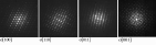
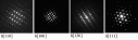
Figure 3. Various electron diffraction patterns from
s-Nb2Al (tetragonal) and d-Nb3Al (cubic) phases.
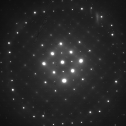


Figure 4. Electron diffraction patterns produced through variation of the lens and aperture systems to determine crystal symmetry and space group for Al2Ti


Figure 5. Electron diffraction used to determine orientation relationship of the Ti2AlNb (O) phase precipitate in Nb solid-solution (
bo).

Figure 6. {221} type twinning in Ti2AlNb

Figure 7. Convergent beam electron diffraction (CBED) pattern of Ti2AlNb. Different intensities are associated with the species of atoms located on that particular plane in the crystal.

Figure 8. Image of anti-phase domains in an ordered phase produced through dark-field imaging using the (100) superlattice reflection.

Figure 9. Image of stacking faults in
s-Nb2Al using the (401) reflection.

Figure 10. Ti2AlNb precipitates clearly illustrated when image is produced with a diffracted beam from the precipitate only.
Kikuchi Diffraction:
A line pattern representing the reciprocal image of the stereographic projection, that is produced from both elastic and inelastic scattering of the electron beam (Figure 11). The lines represent planes in the sample which have diffracted the election beam and intersect each other at particular crystallographic zones. When the incident electron beam strikes the sample, some elastic scattering occurs (diffraction) off of planes oriented to the Bragg angle of the incident beam. In addition, some inelastic scattering also occurs throughout the sample and in all directions (Figure 12). The inelastic scattered electrons may be oriented to the Bragg angle of other planes in the crystal and diffract off of them. The energy loss in the inelastic scattering is small in comparison to the incident electron energy. The diffracted beams, whether they are directly or indirectly scattered from the incident electron beam, produce diffracted cones off of the planes which are diffracting (Kossel cones) which intersects the Ewald’s sphere producing the Kikuchi lines. The Kikuchi lines are actually curved, but due to the small wavelength of the electron beam the Bragg angles are small and the lines appear straight.
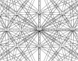
Figure 11. Example of a Kikuchi map near the [101] zone of the tetragonal TiAl phase.
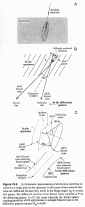
Figure 12. Illustration of Kikuchi line formation.